A study by Brazilian and Portuguese researchers presents the challenges and potentials of green laser-induced graphene (gLIG). gLIG can be extracted from several natural sources of carbon such as leaves, scrap wood, cork and coal. Discoveries pave the way for the generation of green scalable low-cost electronics. The technology will allow the development of wearable and even edible electronic materials. Advance will promote the mitigation of one of the biggest current challenges in environmental sustainability: e-waste. As it is lightweight, flexible, almost transparent, an excellent heat and electricity conductor and about 200 times stronger than steel, graphene is considered a material that can cause a technological revolution in the electronics industry. Among the challenges for its development and applications is producing it from renewable sources. This can be achieved through green laser-induced graphene (gLIG) technology, which was the focus of a study published in the journal Applied Physics Reviews, authored by Brazilian and Portuguese scientists. This technology paves the way for the fabrication of simple, sustainable, low-cost devices based on abundant and renewable carbon sources like wood, leaves, cork, bark and cellulose. Hence it will contribute to the reduction of electronic waste, also known as computational waste or e-waste (see table below). These terms are used to designate devices that are powered by electricity or batteries. Laser-induced graphene (LIG) opens up the possibility of simple, economical and scalable production of technological components,” reports materials engineer Pedro Ivo Cunha Claro, one of the authors of the paper written during his postgraduate studies at the University of São Carlos (UFSCar) and the NOVA University of Lisbon (UNL). The researcher recalls that recent years have seen increasingly more extensive research on green laser-induced graphene (gLIG) for integration into several electronic applications such as supercapacitors, sensors, electrocatalysts and triboelectric nanogenerators. Laser-assisted processing techniques have emerged as powerful tools for a multitude of applications ranging from material processing to device manufacturing,” states Claro, who is currently a Technological Development analyst at the Brazilian Center for Energy and Materials Research (CNPEM) in Campinas, SP. According to him, several gLIG-based systems for energy storage, electrocatalysis, water treatment and sensors have been reported in the literature. In addition, gLIG has been proposed to formulate dyes or to be incorporated into polymer matrices, in order to further expand its use to non-carbon-based substrates or applications where the original Lig cannot be used directly. “Its mechanical and physicochemical properties, such as high mechanical strength capacity and electrical conductivity, make it a material with enormous potential technological applicability in several areas,” the engineer states. Less e-waste The gLIG can spark a revolution in the way integrated circuits and electronic components are produced. With that, the technology will be able to reduce electronic waste, which harms both the environment and human health as it contains toxic additives or dangerous substances such as mercury. The process of obtaining the gLIG itself is cleaner, as it does not use toxic reagents or traditional methods. In 2019, e-waste reached a record 53.6 million metric tons globally, a 21% increase over five years, according to the third edition of the United Nations' Global E-waste Monitor 2020. Brazil leads the generation of electronic waste among Portuguese-speaking nations with 2,141 tons (read here). In addition to Pedro Claro, the paper was authored by Embrapa Instrumentation researchers Luiz Henrique Capparelli Mattoso and José Manoel Marconcini, and by Nova University of Lisbon (UNL) professor Elvira Maria Fortunato, current Minister of Science, Technology and Higher Education of Portugal (see the full list of authors at the end of this news article). Mattoso, who advised Claro at Embrapa's National Laboratory of Nanotechnology for Agribusiness (LNNA) in São Carlos, SP, says the recent discoveries pave the way for the preparation of scalable and low-cost green electronics. “It is possible to apply gLIG on different substrates, aiming at the development of edible and wearable electronic materials. The gLIG can be extracted from wood scraps, leaves, cork and coal, and other natural sources, allowing the development of flexible and sustainable platforms as an alternative to conventional technologies”, states the researcher, who specializes in nanotechnology. “We were able to use LIG technology to design graphene-based circuits by converting carbon chains that are associated with any biopolymer or cellulosic material, which translates into a huge improvement in the resources needed to develop sustainable bioelectronics that contribute to citizens' well-being and comfort,” reports the coordinator of UNL's Materials Research Center (Cenimat), Rodrigo Martins, who also participated in the study. Cork, wood and even leaves can be raw material Mattoso, who was responsible for introducing nanotechnology and studies with new materials in Brazilian agriculture, explains that cork (cork oak tree bark) is a substrate that has aroused a lot of interest and is considered a promising source of gLIG, due to the possibility of being a hybrid material that allows flexibility and lightness. Claro says that such substrates can be converted directly into gLIG, especially due to the high lignin content present in their composition. The scientist clarifies that higher lignin content is more conducive to producing higher-quality gLIG given the possibility of selecting the most suitable raw precursor for each target application, and of adapting the chemical and conductive functions of the resulting gLIG patterns. “From an environmental and economic point of view, such means can be one of the most versatile materials in nature, with extraordinary intrinsic characteristics like biodegradability, impermeability, lightness and resistance to different thermal conditions, providing new functionalities on top of their already consolidated use in the manufacture of wine stoppers”, Claro details. Meanwhile wood has the potential to produce gLIG due to its uniform and smooth surface, which allows for easy standardization of different architectures of electrodes. However, its applicability is limited due to the rigidity and decomposition of the lignocellulosic structure after the laser scan. Nevertheless, it shows great promise for electronic devices that do not have major mechanical requirements. Another natural source of raw materials pointed out by the researcher is coal, an organic sedimentary rock that is rich in carbon and is produced by the compacting and hardening of altered plant remains. Plant leaves could in turn be applied to wearable devices, but their processability is limited by their size and mechanical strength, as well as due to degradation over time. Processed byproducts Marconcini recalls that recent efforts have been made to produce LIG from other carbon-based substrates sourced from a variety of materials ranging from thermoplastic polymers to textile materials and foods, such as potato skins, bread and coconut shells. The versatility and potential of such materials have already been demonstrated in several applications. Graphene and gLIG The thinnest material in the world, graphene is produced from graphite; it is a two-dimensional crystal formed by bonds between carbon atoms, arranged in hexagonal structures resembling a honeycomb. Meanwhile gLIG is an emerging and highly sustainable material, obtained by a technique called laser direct writing (LDW) - three-dimensional (3D) manufacturing from natural substrates that offers significant geometric versatility that reaches micrometric length scales. This new technology is developed at room temperature, without any type of reagent, while conventional graphene is produced at high temperatures, around a thousand degrees centigrade, using very expensive and complex equipment. The elimination of chemical treatments ensures high conversion efficiency, minimizing time and energy consumption in the engraving process. Laser direct writing (LDW), as it is known, is a maskless, catalyst-free, nontoxic, controllable and non-contact approach method, which allows fast, direct and efficient processing of complex structures. This technique resembles a type of etching based on photothermal reactions, transforming the etched surface into a material of technological interest. Perspectives Since its discovery in 2004, graphene and similar two-dimensional (2D) nanomaterials have been intensely studied and attracted much interest due to their promising physicochemical properties, as some products are already commercially available and have shown promising performances compared to other green sources. The European Union has created a consortium, the Graphene Flagship, composed of 150 partners with a total budget of 1 billion euros. The project covers several fields ranging from basic research to long-term graphene trading. Similar efforts, aimed at fully unraveling and exploiting the properties of graphene, are being carried out around the world, including in Brazil, a major graphite producer and holder of one of the world's largest reserves of the mineral. To date, graphene has been successfully used in energy storage, environmental and biomedical applications, among others. For Mattoso, although there are many challenges to overcome, there are opportunities for different processing methods, materials and products to enter the market, as graphene is a versatile material and can be combined with other elements to produce different materials with superior properties. In addition to all of such advantages, gLIG can also contribute to the UN Sustainable Development Goals (SDGs). Authors The authors of the paper are Pedro Claro (UFSCar); Tomás Pinheiro, Sara L. Silvestre, Ana C. Marques, João Coelho, Rodrigo Martins Elvira Fortunato (Nova University of Lisbon); Luiz H. C. Mattoso and José M. Marconcini (Embrapa). The study was partially funded by the Coordination for the Improvement of Higher Education Personnel (Capes) and the National System of Nanotechnology Laboratories (SisNano). The Project had financial support from the European Research Council (ERC) and from Portugal’s National Foundation for Science and Technology (FCT).
Photo: Pedro Ivo

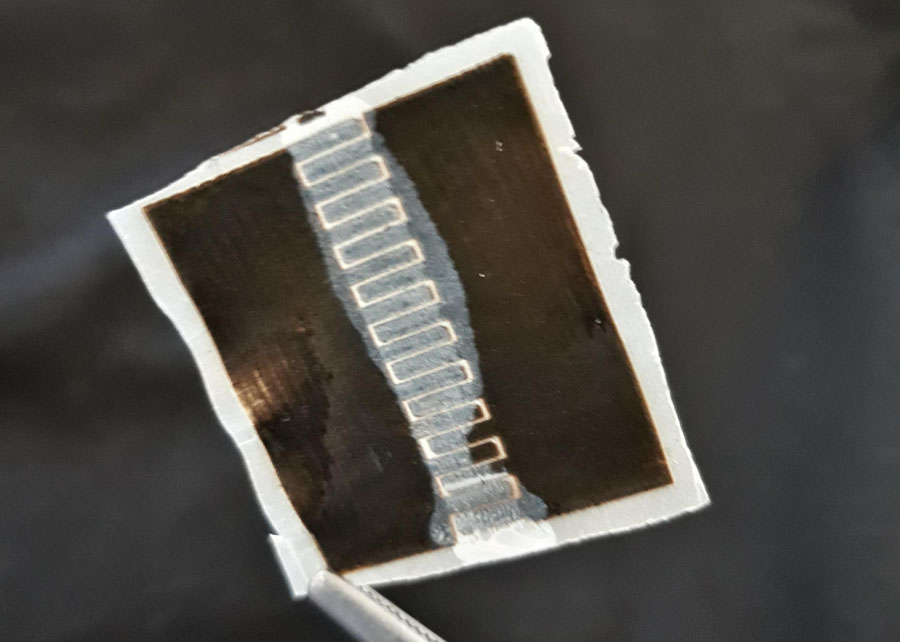
UV sensor developed by laser graphitizing pineapple cellulose nanocrystals
As it is lightweight, flexible, almost transparent, an excellent heat and electricity conductor and about 200 times stronger than steel, graphene is considered a material that can cause a technological revolution in the electronics industry. Among the challenges for its development and applications is producing it from renewable sources. This can be achieved through green laser-induced graphene (gLIG) technology, which was the focus of a study published in the journal Applied Physics Reviews, authored by Brazilian and Portuguese scientists.
This technology paves the way for the fabrication of simple, sustainable, low-cost devices based on abundant and renewable carbon sources like wood, leaves, cork, bark and cellulose. Hence it will contribute to the reduction of electronic waste, also known as computational waste or e-waste (see table below). These terms are used to designate devices that are powered by electricity or batteries.
Laser-induced graphene (LIG) opens up the possibility of simple, economical and scalable production of technological components,” reports materials engineer Pedro Ivo Cunha Claro, one of the authors of the paper written during his postgraduate studies at the University of São Carlos (UFSCar) and the NOVA University of Lisbon (UNL). The researcher recalls that recent years have seen increasingly more extensive research on green laser-induced graphene (gLIG) for integration into several electronic applications such as supercapacitors, sensors, electrocatalysts and triboelectric nanogenerators.
Laser-assisted processing techniques have emerged as powerful tools for a multitude of applications ranging from material processing to device manufacturing,” states Claro, who is currently a Technological Development analyst at the Brazilian Center for Energy and Materials Research (CNPEM) in Campinas, SP.
According to him, several gLIG-based systems for energy storage, electrocatalysis, water treatment and sensors have been reported in the literature. In addition, gLIG has been proposed to formulate dyes or to be incorporated into polymer matrices, in order to further expand its use to non-carbon-based substrates or applications where the original Lig cannot be used directly.
“Its mechanical and physicochemical properties, such as high mechanical strength capacity and electrical conductivity, make it a material with enormous potential technological applicability in several areas,” the engineer states.
| The gLIG can spark a revolution in the way integrated circuits and electronic components are produced. With that, the technology will be able to reduce electronic waste, which harms both the environment and human health as it contains toxic additives or dangerous substances such as mercury. The process of obtaining the gLIG itself is cleaner, as it does not use toxic reagents or traditional methods. In 2019, e-waste reached a record 53.6 million metric tons globally, a 21% increase over five years, according to the third edition of the United Nations' Global E-waste Monitor 2020. Brazil leads the generation of electronic waste among Portuguese-speaking nations with 2,141 tons (read here). |
 In addition to Pedro Claro, the paper was authored by Embrapa Instrumentation researchers Luiz Henrique Capparelli Mattoso and José Manoel Marconcini, and by Nova University of Lisbon (UNL) professor Elvira Maria Fortunato, current Minister of Science, Technology and Higher Education of Portugal (see the full list of authors at the end of this news article).
Mattoso, who advised Claro at Embrapa's National Laboratory of Nanotechnology for Agribusiness (LNNA) in São Carlos, SP, says the recent discoveries pave the way for the preparation of scalable and low-cost green electronics. “It is possible to apply gLIG on different substrates, aiming at the development of edible and wearable electronic materials. The gLIG can be extracted from wood scraps, leaves, cork and coal, and other natural sources, allowing the development of flexible and sustainable platforms as an alternative to conventional technologies”, states the researcher, who specializes in nanotechnology.
“We were able to use LIG technology to design graphene-based circuits by converting carbon chains that are associated with any biopolymer or cellulosic material, which translates into a huge improvement in the resources needed to develop sustainable bioelectronics that contribute to citizens' well-being and comfort,” reports the coordinator of UNL's Materials Research Center (Cenimat), Rodrigo Martins, who also participated in the study.
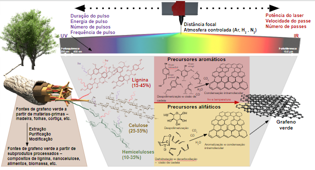
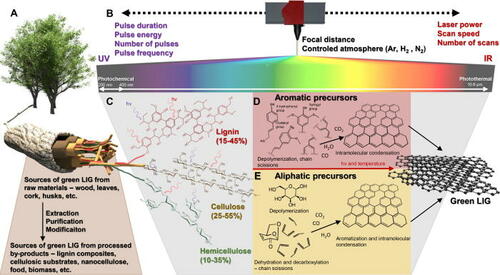
Cork, wood and even leaves can be raw material Mattoso, who was responsible for introducing nanotechnology and studies with new materials in Brazilian agriculture, explains that cork (cork oak tree bark) is a substrate that has aroused a lot of interest and is considered a promising source of gLIG, due to the possibility of being a hybrid material that allows flexibility and lightness. Claro says that such substrates can be converted directly into gLIG, especially due to the high lignin content present in their composition. The scientist clarifies that higher lignin content is more conducive to producing higher-quality gLIG given the possibility of selecting the most suitable raw precursor for each target application, and of adapting the chemical and conductive functions of the resulting gLIG patterns. “From an environmental and economic point of view, such means can be one of the most versatile materials in nature, with extraordinary intrinsic characteristics like biodegradability, impermeability, lightness and resistance to different thermal conditions, providing new functionalities on top of their already consolidated use in the manufacture of wine stoppers”, Claro details.
Meanwhile wood has the potential to produce gLIG due to its uniform and smooth surface, which allows for easy standardization of different architectures of electrodes. However, its applicability is limited due to the rigidity and decomposition of the lignocellulosic structure after the laser scan. Nevertheless, it shows great promise for electronic devices that do not have major mechanical requirements. Another natural source of raw materials pointed out by the researcher is coal, an organic sedimentary rock that is rich in carbon and is produced by the compacting and hardening of altered plant remains. Plant leaves could in turn be applied to wearable devices, but their processability is limited by their size and mechanical strength, as well as due to degradation over time. Processed byproducts Marconcini recalls that recent efforts have been made to produce LIG from other carbon-based substrates sourced from a variety of materials ranging from thermoplastic polymers to textile materials and foods, such as potato skins, bread and coconut shells. The versatility and potential of such materials have already been demonstrated in several applications. |
 Graphene and gLIG Graphene and gLIG
The thinnest material in the world, graphene is produced from graphite; it is a two-dimensional crystal formed by bonds between carbon atoms, arranged in hexagonal structures resembling a honeycomb. Meanwhile gLIG is an emerging and highly sustainable material, obtained by a technique called laser direct writing (LDW) - three-dimensional (3D) manufacturing from natural substrates that offers significant geometric versatility that reaches micrometric length scales. This new technology is developed at room temperature, without any type of reagent, while conventional graphene is produced at high temperatures, around a thousand degrees centigrade, using very expensive and complex equipment. The elimination of chemical treatments ensures high conversion efficiency, minimizing time and energy consumption in the engraving process. Laser direct writing (LDW), as it is known, is a maskless, catalyst-free, nontoxic, controllable and non-contact approach method, which allows fast, direct and efficient processing of complex structures. This technique resembles a type of etching based on photothermal reactions, transforming the etched surface into a material of technological interest. |
Perspectives
Since its discovery in 2004, graphene and similar two-dimensional (2D) nanomaterials have been intensely studied and attracted much interest due to their promising physicochemical properties, as some products are already commercially available and have shown promising performances compared to other green sources.
The European Union has created a consortium, the Graphene Flagship, composed of 150 partners with a total budget of 1 billion euros. The project covers several fields ranging from basic research to long-term graphene trading.
Similar efforts, aimed at fully unraveling and exploiting the properties of graphene, are being carried out around the world, including in Brazil, a major graphite producer and holder of one of the world's largest reserves of the mineral. To date, graphene has been successfully used in energy storage, environmental and biomedical applications, among others.
For Mattoso, although there are many challenges to overcome, there are opportunities for different processing methods, materials and products to enter the market, as graphene is a versatile material and can be combined with other elements to produce different materials with superior properties. In addition to all of such advantages, gLIG can also contribute to the UN Sustainable Development Goals (SDGs).
Authors The authors of the paper are Pedro Claro (UFSCar); Tomás Pinheiro, Sara L. Silvestre, Ana C. Marques, João Coelho, Rodrigo Martins Elvira Fortunato (Nova University of Lisbon); Luiz H. C. Mattoso and José M. Marconcini (Embrapa). The study was partially funded by the Coordination for the Improvement of Higher Education Personnel (Capes) and the National System of Nanotechnology Laboratories (SisNano). The Project had financial support from the European Research Council (ERC) and from Portugal’s National Foundation for Science and Technology (FCT). |
Joana Silva (MTb 19.554/SP)
Embrapa Instrumentation
Press inquiries
instrumentacao.imprensa@embrapa.br
Phone number: +55 16 2107 2901/ 99994.6160
Translation: Mariana Medeiros (13044/DF)
Superintendency of Communications
Further information on the topic
Citizen Attention Service (SAC)
www.embrapa.br/contact-us/sac/
 In addition to Pedro Claro, the paper was authored by Embrapa Instrumentation researchers Luiz Henrique Capparelli Mattoso and José Manoel Marconcini, and by Nova University of Lisbon (UNL) professor Elvira Maria Fortunato, current Minister of Science, Technology and Higher Education of Portugal (see the full list of authors at the end of this news article).